Introduction
This article presents several circuits that may be used to apply the Memory Bank as a Read/Write memory, commonly called RAM. It assumes that the memory will be attached to a common data bus for input and output. This means there must be a way to tell this circuit two things – when the data on the bus is for it, and when to output its data to another device. We still need the proper controls for the clock input to the bank as well.
When the bank is used as Read/Write memory, we must use the clock input. That means we have to deal with the ‘weirdness’ of this input. In addition to this input serving two functions, it is also edge-triggered, rather than level sensitive. That means the timing of the changes must be considered in relationship to the system timing needs.
The clock input can be derived different ways depending on what control signals are available from the system. There must be at least one signal that tells it what type of access to initiate and perhaps another one that sets the timing of the access. In order to be connected to the bus, there must also be an output enable as well. These signals control data bus access and must be timed correctly for the bus interface.
As is typical in any clocked system, all the address lines, the R/-W control, any other control signals and any data that must be read from the data bus are set to their required levels and allowed to settle first. Then the system clock transitions (usually to ‘1’) to initiate any action.
Example Circuits
The following circuits show only one slice of data memory or one ‘nibble’ (4bits). Most systems need a larger data size. The dotted box shows the portions that need to be repeated for the rest of the data bus. All control and address lines are common between these slices. Only the data I/O is separate. There are portions of circuitry needed but not shown. That is because those circuits are dependent on the system’s architecture and may be different for each system. These examples attempt to cover the needs of the vast majority of system architectures, however. The memory bank labeled ‘( )’ is the actual memory store. This label is used to indicate that it is not pre-programmed. All other banks shown are used as programmed logic devices, or PLDs. Each example gives the program needed, when possible. If the PLD is used as a memory space decoder, as in example 2, it must be programmed so its output only goes high with the required input values. Since these values are determined by the system architecture, no example program can be given. If they input assignments must be changed from that shown then the given program cannot be used and must be ‘inverted’ first. That does not mean a logical inversion, but a matrix inversion. See mathematical textbooks or websites for an explanation.
Example 1
The first circuit is likely the most commonly used design in a system. The circuit uses a general R/-W line and a modified select line – the SelClk signal. This signal contains both the timing requirement and the device selection – a form of address decoding. These two controls then hold all the information the memory bank needs to operate properly and in time. However, the voltage levels still need to be converted to the levels the bank requires. This circuit uses a second bank labeled ‘VC’ for voltage converter. It also combines the two controls for the proper timing.
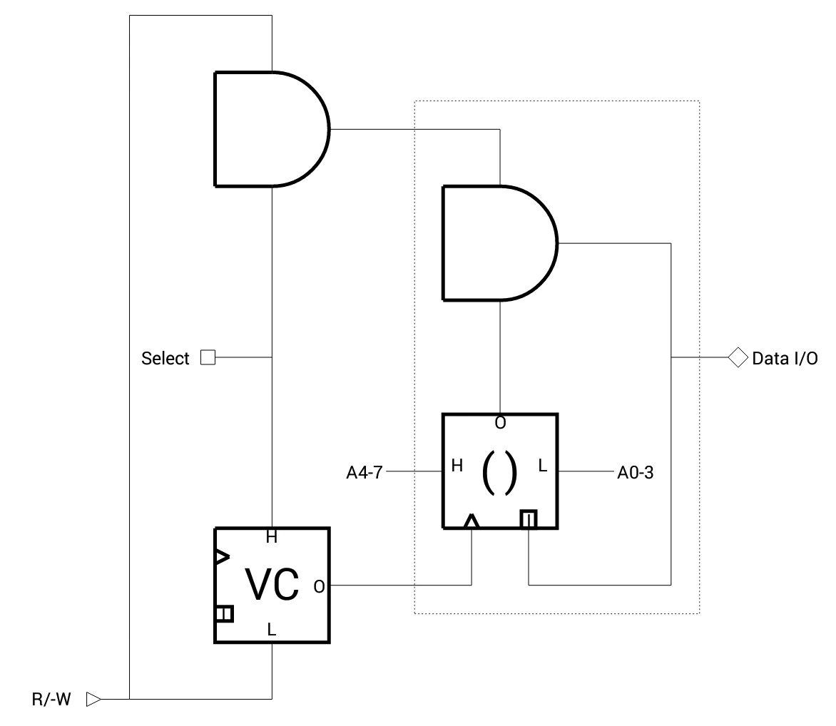
The PLD ‘VC’ only needs programming in the last row (‘F’): 400000000000000F (To invert this matrix, put that data down the ‘F’ column, with the ‘4’ at the top.)
Example 2
This is a more complete diagram which includes an example address decoding scheme. The higher order addresses are decoded with a memory bank used as a demultiplexer labeled ‘Dec’. Each decoder bank must be programmed to respond only to the proper memory block location. It is further assumed that the memory is not accessed with every clock cycle so there is also a Memory Select control line provided by the system. This is a global control and is ANDed with the system clock to provide a timed Memory Clock signal, MemClk. This signal would be common to the entire memory array. It is then ANDed with the decoded memory space to provide the local chip select, SelClk. The rest of the circuit is identical to example 1.
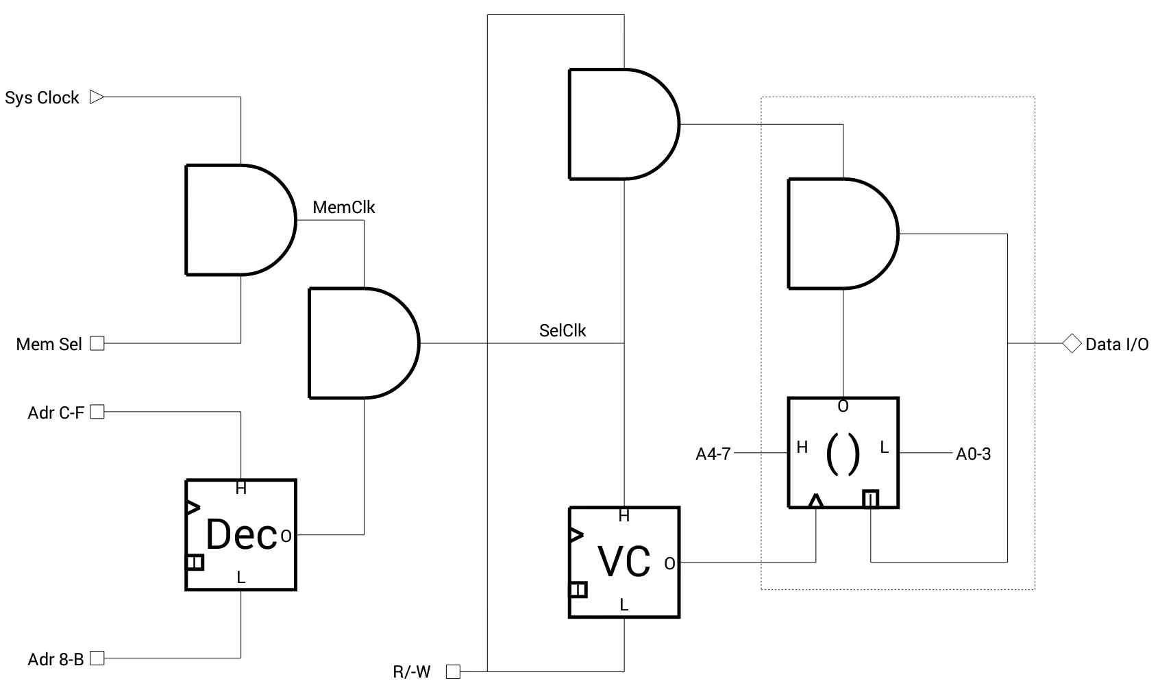
The decoding scheme shown above can be used in the following circuits as well, with some modifications. There are also many other ways to generate the SelClk control. Further details will not be shown as they depend on the overall system design. The PLD ‘VC’ only needs programming in the last row (‘F’): 400000000000000F The PLD ‘Dec’ must be programmed according to the system architecture but it will hold an ‘F’ in the one location corresponding to where this memory block is located in the global memory space.
Example 3
Two separate Read and Write signals may be supplied by the system. In this example they already have the selection and timing requirements built in. Thus they only go active (to ‘1’) when access to or from this particular RAM block is requested. Both the Read and Write controls must return to ‘0’ before a new memory access cycle can be initiated. They only need to be combined and set to the right voltages for the bank’s clock input. This is accomplished with another memory bank called ‘VC’ in the diagram.
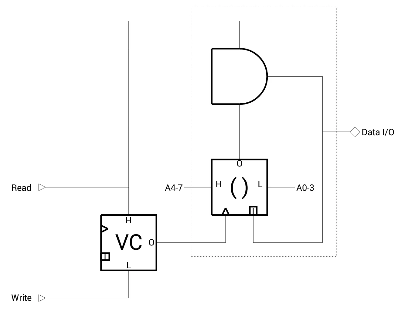
The PLD ‘VC’ is programmed with: 000000000000000400000000000000000000000000000000000000000000000000000000000000000000000000000000000000000000000000000000000000000000000000000000000000000000000000000000000000000000000000000000000000000000000000000000000000000000000000000000F000000000000000
Both the Read and Write controls should never be active at the same time. This program will abort any access if this happens, to help ensure data integrity in the bank. (To invert this matrix, simply swap the ‘4’ and the ‘F’.)
Example 4
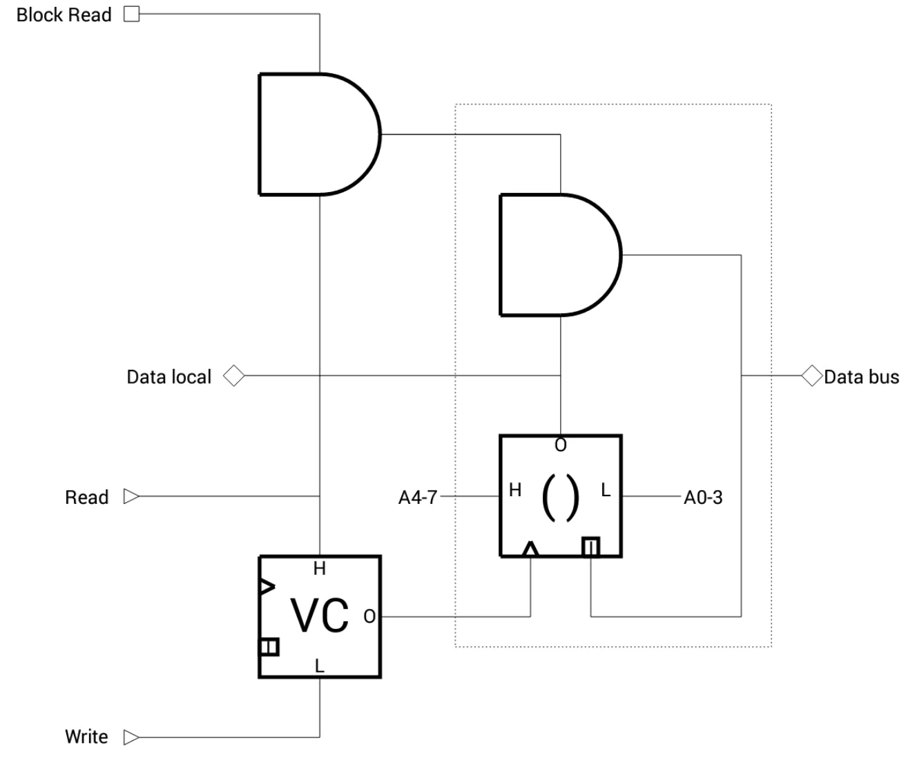
The system design may require a memory section to provide a local output that stays active even without being connected to the data bus. This might be to supply data to an output device while allowing the system to read and write the data. That data may not always be needed on the bus and yet sometimes will have to be read by the system. There are many possibilities with this feature that cannot be detailed here but this example will give you the basic idea of how to accomplish them. The bank’s clock input may be derived by one of the means above. This example is similar to the last one but has a separated output enable control that is not constantly tied into the memory read control. Instead, it includes a Block Read control that only allows the circuit to output to the data bus under certain conditions. These conditions will be specific to the architecture and cannot be detailed further here.

The PLD ‘VC’ is programmed identical to the one above. This circuit does assume that all writes to the memory block will be done via the data bus and that all reads are controlled by the central system. That may not always be the case and dual control of the memory’s access will be required. Such control can be accomplished with multiplexers for the Read and Write control lines but the timing of these controls must be carefully considered and is beyond the scope of this article.